
OUR NEW VIEW AND APPROACHES FOR
FLEXIBLE ELECTRONICS.
The additive technology allows to produce the adhesiveless metal clad laminates and precise FPCB, highly sensitive flexible sensor systems and new generation of the FE & FHE wearable devices.Having used our patented solutions and materials, you will have spent significantly less energy, water, chemicals,workspace, equipment, money and time for your own production process.
RIVALTEC is one of the first private R&D projects for the Flexible Electronics materials in the world. Our team has had wide successful experience and deep knowledge for that since 80-th years of the last age.
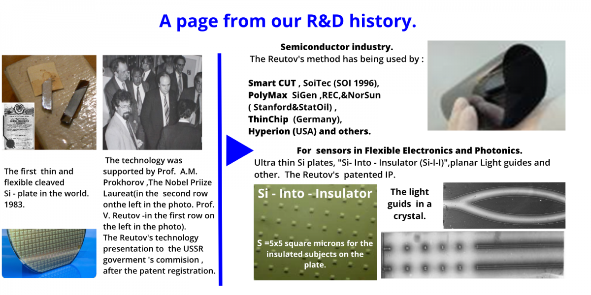
The first our product – ” A method to produce the ultra thin Si-plates with the gas ions implantation” was created and patented in 1983 . It was happenned before (~12 years ) than the “Smart Cut” method, whuch was designed by the SOITEC and ShinEtsu. Our approach is the base part of the technology using for the industral process of the SOI and MEMS production over than 35 years yet.
So, we can offer our solutions to high-tech S&M companies to help them in their own competitive to the global players on the market.
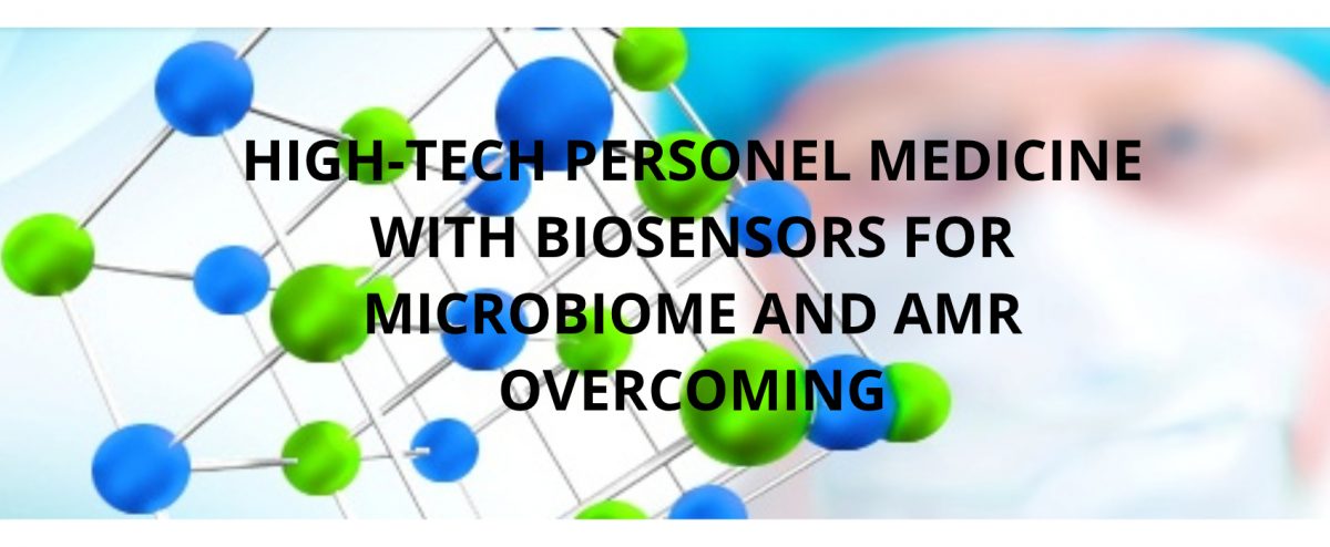
In according to the main market demands to wearable and flexible electronics : miniaturization, cost, reliable, thermal stability, bio compatibility and other, we can propose some of the next our technological solutions for the new generation devices for Industry 4.0.
 1. Flexible Hybrid Electronics (FHE).
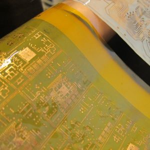
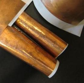
The first direct additive technology for an adhesiveless HDI FPCB (flexible printed circuit board) production. New adhesiveless cooper clad laminates and other adhesiveless metal clad films with complex composite as for a standard technology of the FPCB production as for the new technological demands.
2. Thermal Interface Materials.
The first ultra thin ( 0.1 mm) and flexible thermal pipe and other new TIMs solutions . The sizes of flexible TIMs are possible up to A4 ( 200×300 mm) format for the similar products.
3. Thin semiconductor structures for the sensor systems.
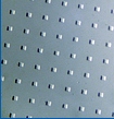
Ultra thin structures “Si into insulator” for flexible electronics (IC, MEMS, sensors).Probably it’s a simplest way to obtain the semiconductor structures for analog and digital sensor systems in the three steps without a clean room and the Fab’s services.
These structures are volume insulated into the Si-wafer. Ones could be with any shapes without the bonding process using. It’s the alternative technical solution to the SOI (Si- on- Insulator technology) for IC, MEMS and NEMS. So, you can create the ultra thin insulated structures on a Si waffer directly.
4. Biocompatible materials and solutions for the medical applications and tools.
Our solutions and new adhesiveless composite materials for biocompatible and implantable electronics and sensor -embeded medical tools. There is an absolutely new level of reliability of the flexible structures of FHE, especially for a dynamic application of different sensors and neuro interface systems as into a human body, as for IVD and other bio-medical applications.
5. Others.
High-tech solutions for IP and BRAND protection.
Smart ID labels with different embedded sensors for the protection against counterfeit.
Bactericidal and biocompatible materials and sensor solutions for bio-medical application, implantable electronics, personal protection of health.
Flexible electronics.
Adhesiveless materials for HDI FPCB, Rigid-Flex PCB. Effective thermal management- TIMs, ultra thin flexible thermal pipes and other.
New opportunites and applications of semiconductor and optical materials in Flexible electronics and sensor systems.


Some of the technological advantages :
-
The additive and adhesiveless technology for a precise FPCB and metal clad laminates production process in the three steps. Z-axis electric conductivity into polymeric film, so there are not any THVs and its drilling and metallization. Cost and time effective process with high ecological standards.
-
A lot of opportunities to creat the novel ultra precise and complex composite, conductive structures and Me -claded materials on a polymeric film carrier for wearable and flexible electronics.
-
Capabilities for the S2S and R2R production process are available.
-
The offered solutions are compatible to all of the standard existed technologies and materials in microelectronics.
-
Biocompatable materials to a human body, ones could be used with other biomaterials and the sensor -embeded medical tools for bio-med industry.
Our motto is “DIES DIEM DOCET” (latin).